Stock Code
301528

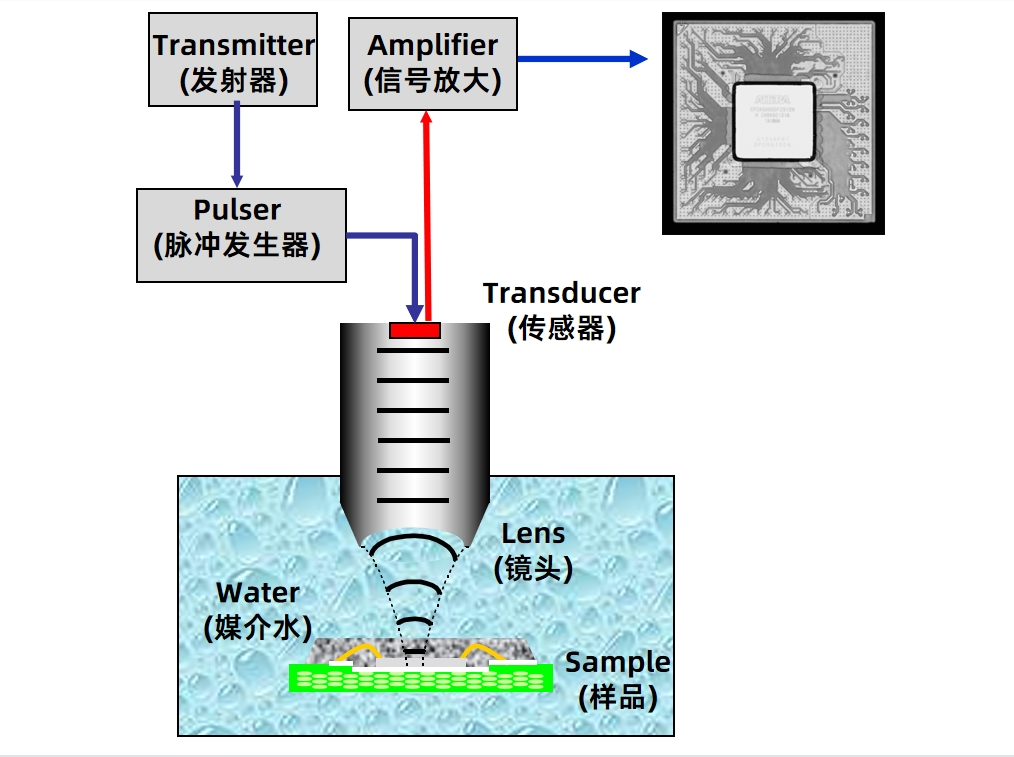
Scanning Acoustic Microscope (SAM) is a non-destructive testing device that uses high-frequency ultrasonic waves to detect the internal structure of samples. Its working principle is as follows: ultrasonic waves are emitted by piezoelectric transducers, focused by acoustic lenses, and transmitted to the sample through coupling media such as water. Reflected or transmitted signals are collected to generate images, enabling layered visualization of micron-scale defects, including delaminations, cracks, voids and more.
This technology features three major application advantages:
① It enables non-destructive testing of multi-layered integrated circuit structures in the microelectronics industry;
② In materials science, it can visualize microscopic features such as grain boundaries without sample polishing;
③ It supports in-vivo tissue observation in the biomedical field.
With versatile imaging modes, SAM penetrates deep into materials and reveals microstructural characteristics at micron resolution, providing accurate and detailed analytical references for researchers and engineering technicians.
Working Principle of SAM
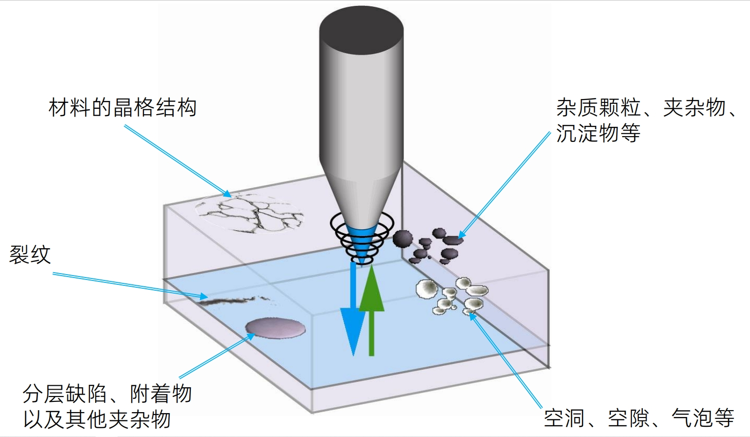
Main Defects Detected by SAM
Doppler Scanning Acoustic Microscope
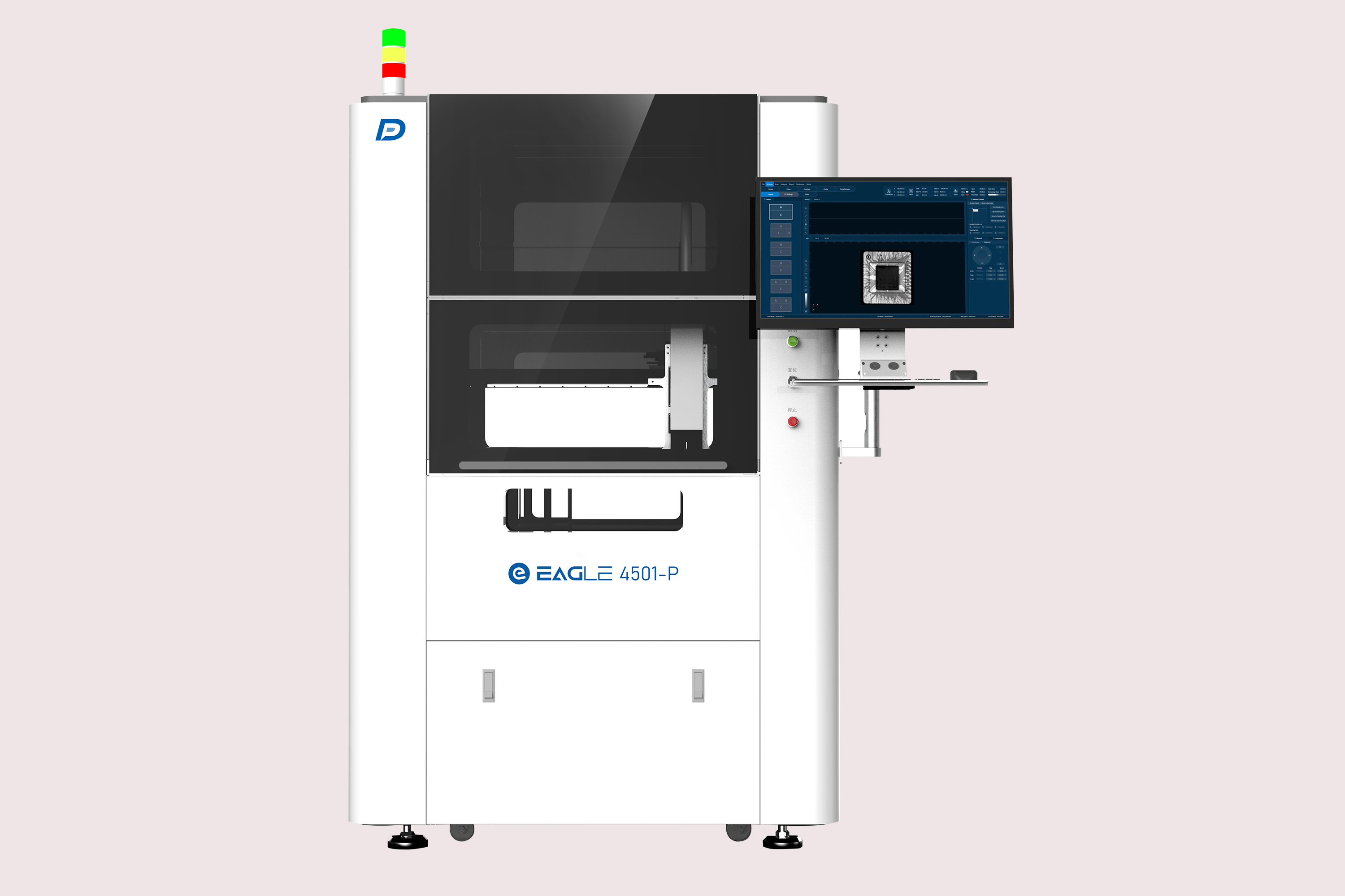
Doppler scanning acoustic microscope is equipped with advanced screening functions, enabling efficient and accurate positioning and locking of target inspection areas, which greatly improves inspection efficiency and accuracy. This feature allows high-volume scanning of multiple similar products within a short time.
Meanwhile, it realizes intelligent defect calculation and recognition, automatically and rapidly capturing various potential defects such as cracks, inclusions and pores. It provides strong support for quality control and failure prevention. This intelligent inspection method not only enhances detection precision, but also significantly reduces misjudgment caused by human factors, bringing revolutionary improvements to scientific research and industrial production.
Software Functions
1. Multi-dimensional Imaging for Comprehensive Control: Supports multiple imaging modes including A-scan, B-scan, C-scan, D-scan and X-scan to accurately display product details. Combined with data marking and waveform comparison, it realizes in-depth tracking and precise analysis of defects.
2. Flexible Skipping for Efficient Inspection: Allows customization of non-scanning areas for individual products to quickly skip unnecessary testing sections, greatly saving inspection time.
3. Tray Scanning for One-stop Testing: Compatible with tray scanning to simultaneously inspect multiple products of the same type at high speed, satisfying mass production testing requirements.
4. Diversified Measurement for Accurate Evaluation: Provides up to 9 manual measurement methods, such as point-to-point distance, parallel width and polyline measurement, to meet diverse measurement demands.
5. Visual Intelligence with Algorithm Import: Enables import of machine vision-based image evaluation algorithms to achieve automatic defect identification and assessment.
6. Manual Framing & Intelligent Calculation: After manually framing defect areas, the system automatically calculates defect size, area and proportion, simplifying the analysis process.
7. Image Export for Intuitive Presentation: A/B/C/D-scan images can be exported in PNG format for clear visualization of inspection results.
8. Multi-format Data Export: A-scan, C-scan and raw data are available for export in Excel and point cloud formats, facilitating subsequent data analysis and secondary application.
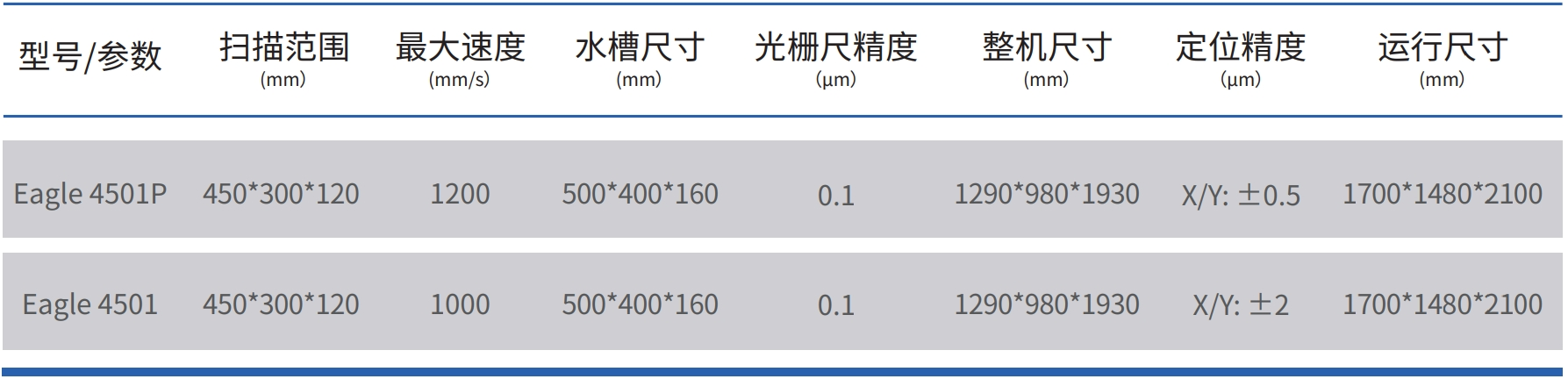
Specifications & Parameters
1.Ultrasonic and Digital Performance
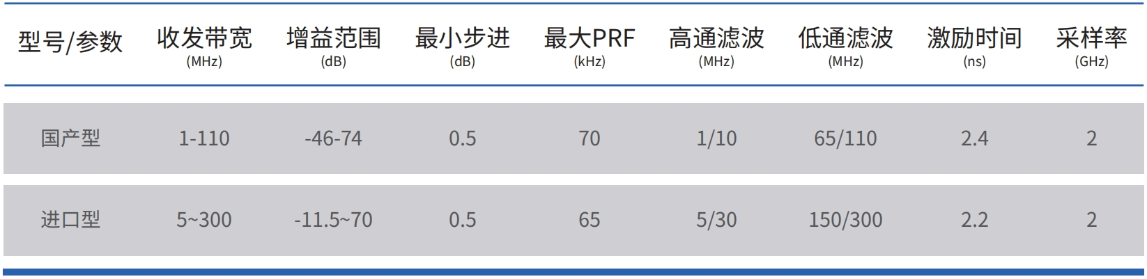
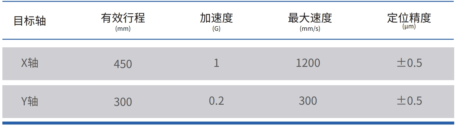
2.Mechanical and Motion System
3.Scanning Platform
Application Cases
1.Multi-Layer Ceramic Capacitor (MLCC)
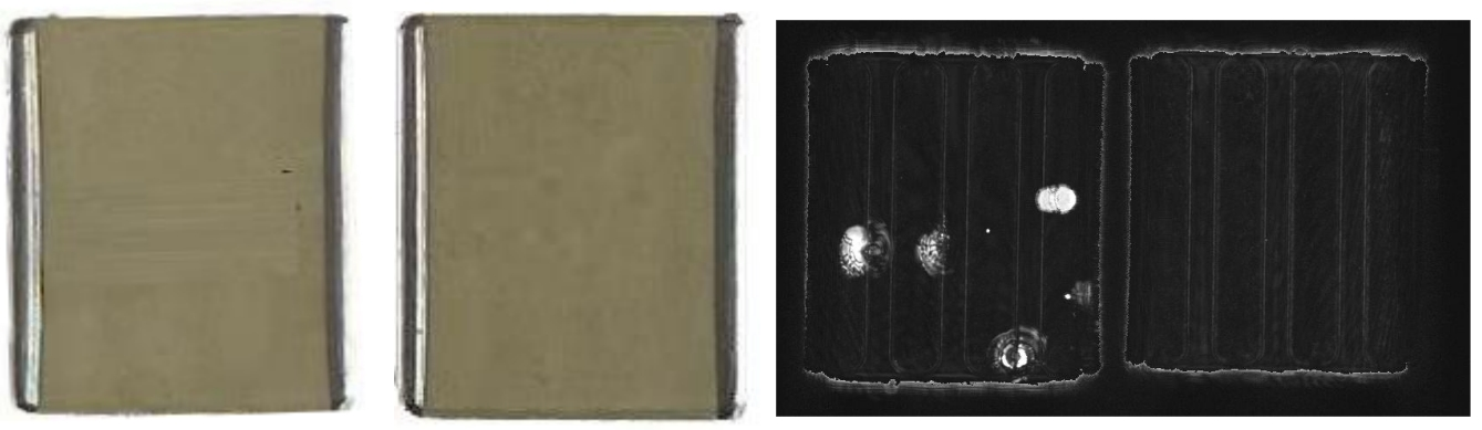
The performance and reliability of multi-layer ceramic capacitors depend on the integrity of their internal structure. The scanning acoustic microscope is capable of detecting micro defects such as interlayer voids and cracks, as well as accurately analyzing the position and size of defects. It provides a scientific basis for quality control and ensures stable operation of MLCCs in complex service environments.
2、Wafer
Wafer bonding technology is critical to chip manufacturing. With high-resolution imaging, the scanning acoustic microscope detects voids, cracks and delaminations at bonding interfaces to deliver comprehensive non-destructive evaluation. It helps manufacturers optimize process parameters and ensure high-yield production of high-density chips.

3、IGBT
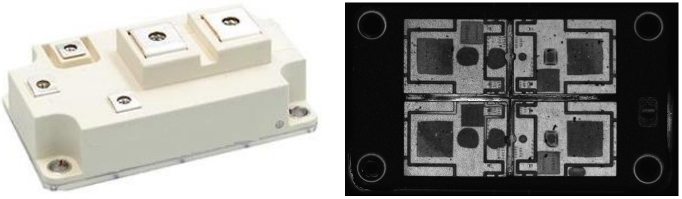
As a core component of power electronics, the welding layer quality and internal structure of IGBT modules directly determine automotive-grade performance. The scanning acoustic microscope enables non-destructive testing of solder layer voids, delaminations and other internal defects, achieving accurate assessment of key risks. It helps manufacturers ensure IGBT modules meet strict high-reliability standards for automotive applications.
4、Ceramic Copper Clad Board (AMB/DBC)
Ceramic copper clad boards, including AMB and DBC types, are widely adopted as core components in power semiconductor modules. The scanning acoustic microscope accurately detects delaminations, voids and other structural defects, delivering comprehensive quality assurance for the high efficiency and reliability of power semiconductors.