Stock Code
301528

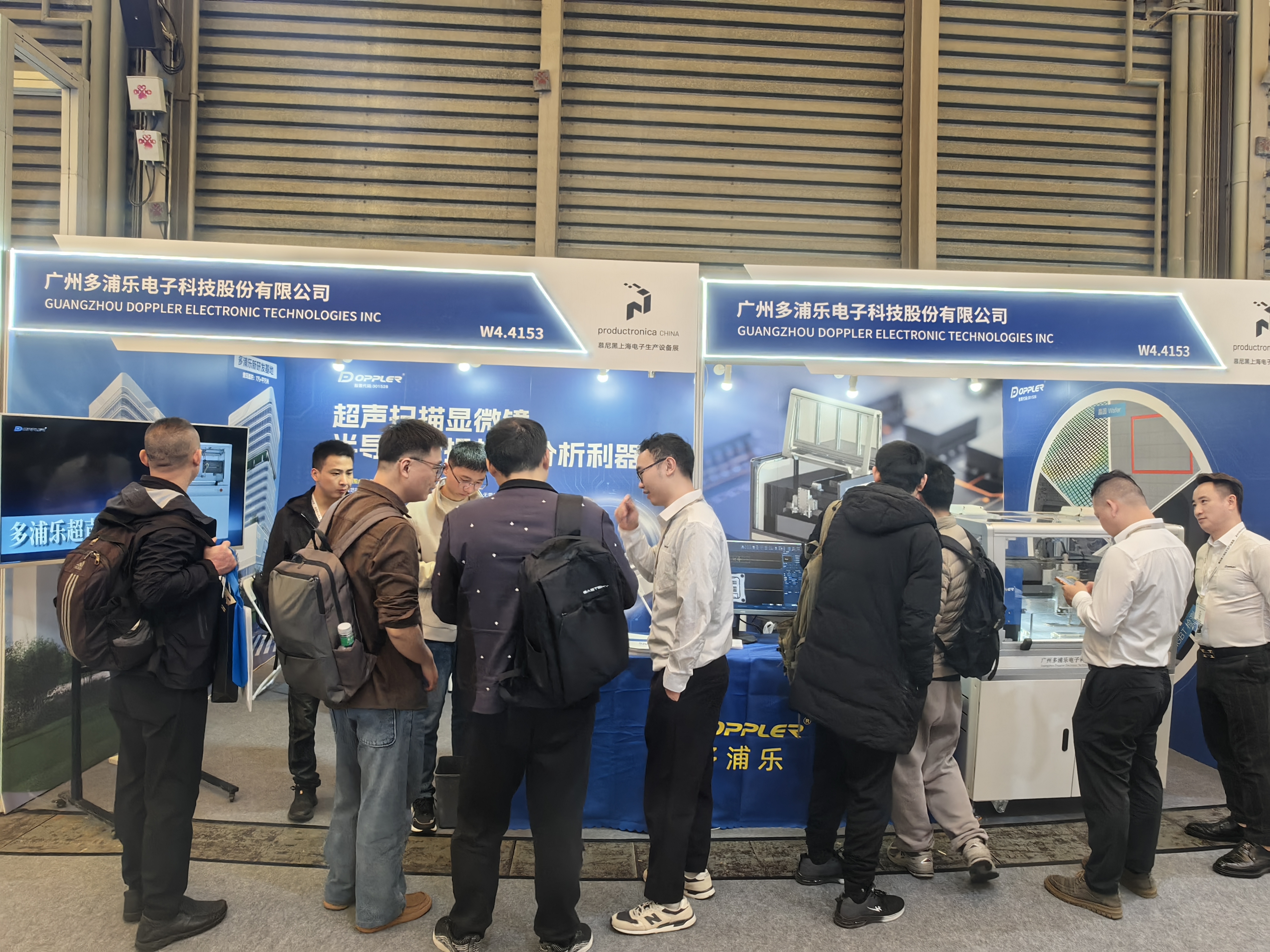
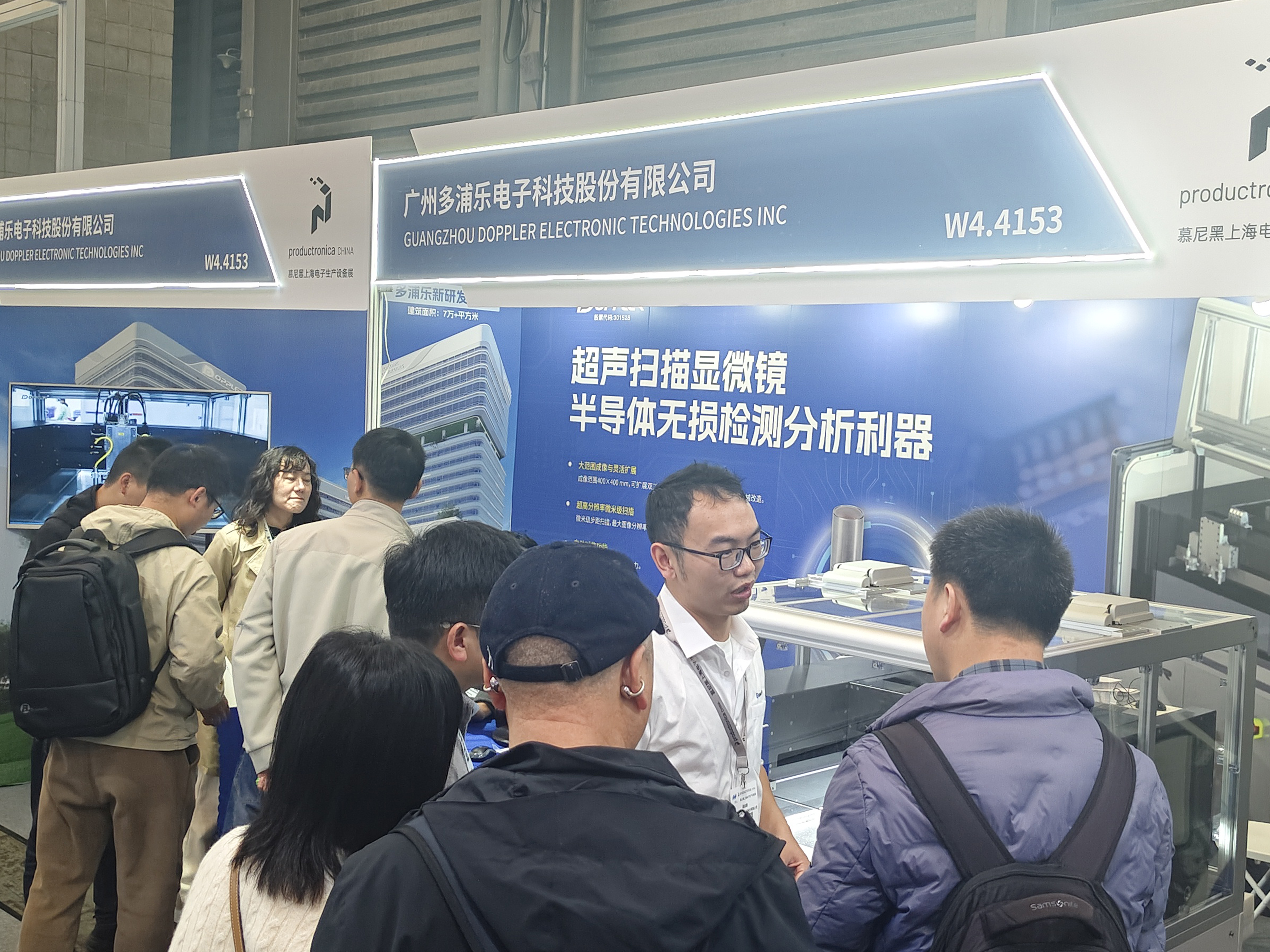
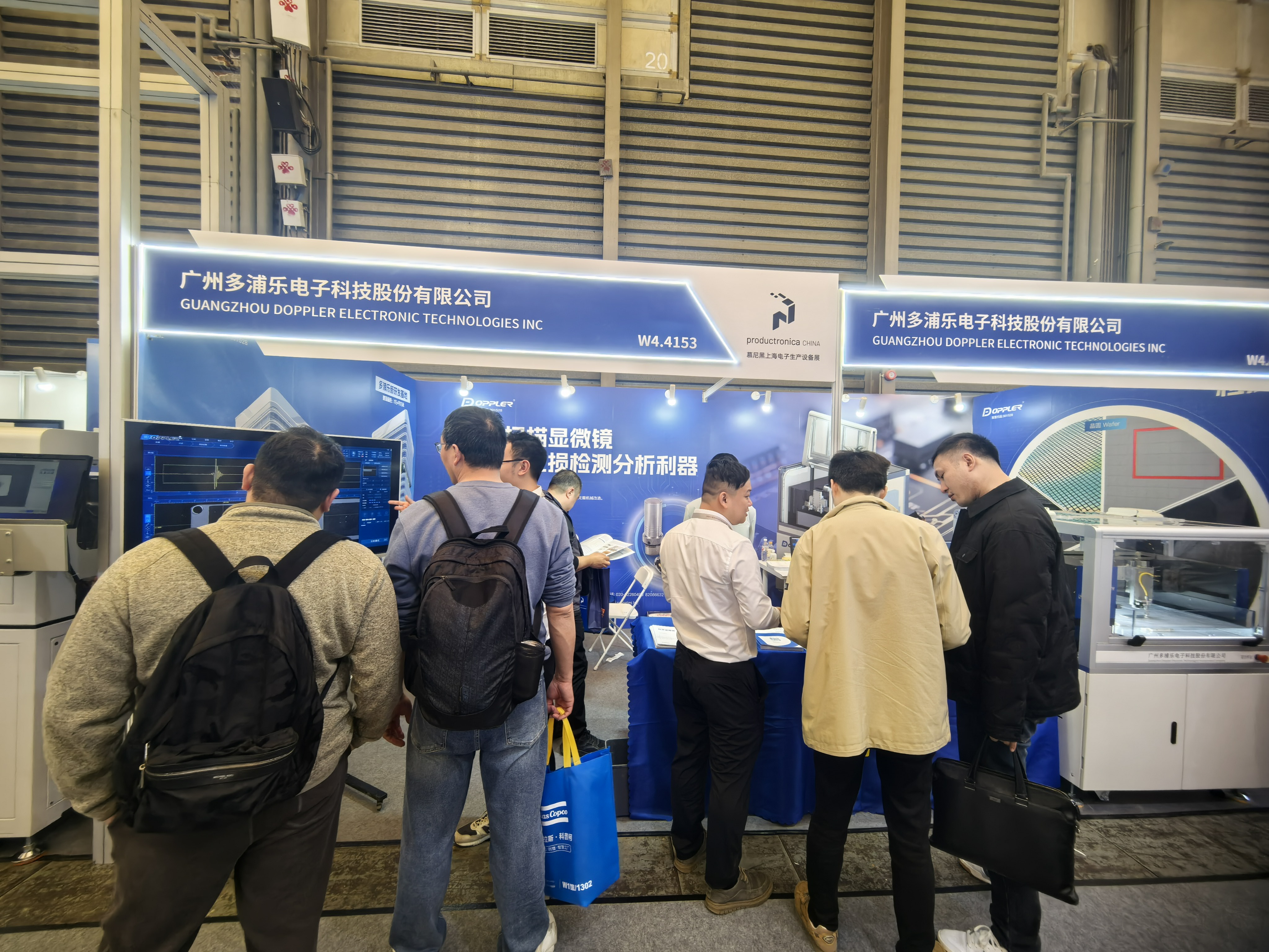
From March 25 to 27, 2026, Doppler showcased its advanced non-destructive testing solutions for semiconductors at productronica China 2026. As a vital exhibition and communication platform for the electronics manufacturing industry, this event gathered cutting-edge global technologies and innovative products.
During the exhibition, Doppler unveiled its self-developed scanning acoustic microscope for the first time, drawing widespread attention from numerous professional visitors. Among them, the 400 Series scanning acoustic microscope won high recognition from on-site guests for its outstanding inspection performance, sophisticated industrial design and excellent cost-performance ratio. Many customers expressed their intentions to submit samples for testing on the spot.
DOPPLER SAM
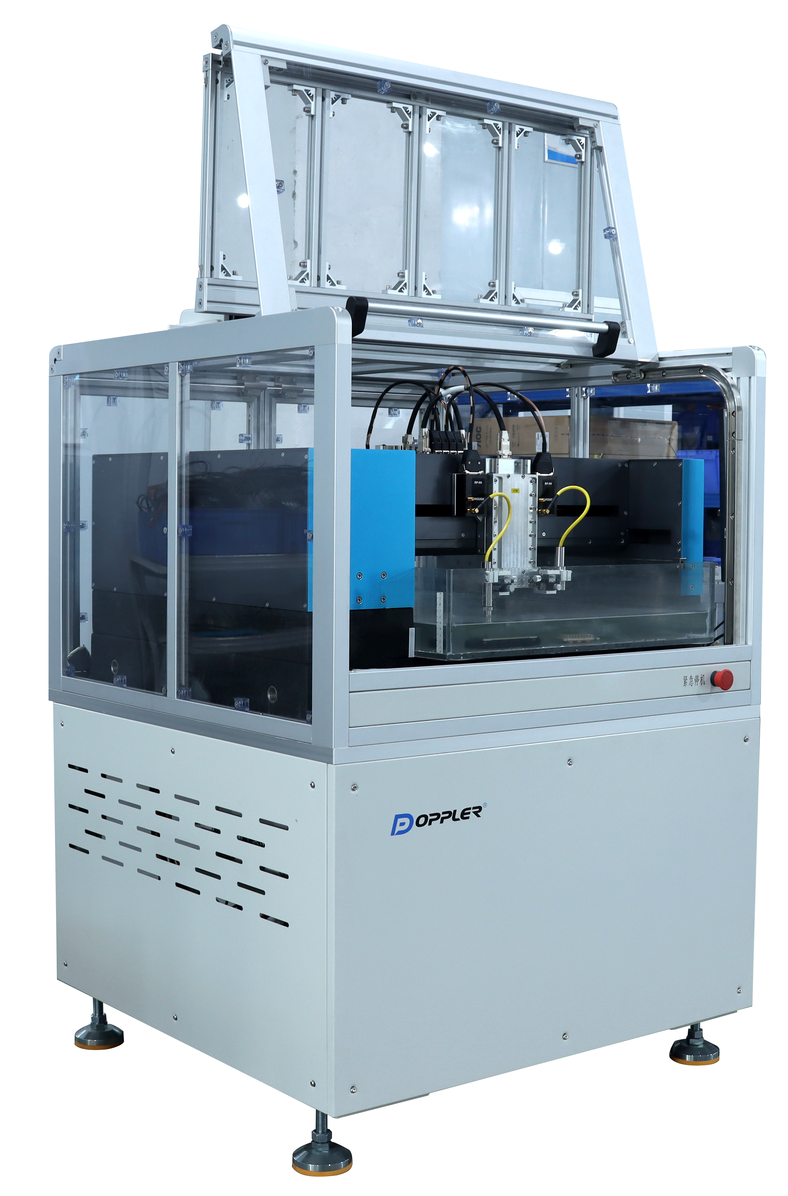
The Doppler Eagle 400 Series Scanning Acoustic Microscope is equipped with advanced screening functions, which can efficiently and accurately locate and lock target inspection areas, greatly improving testing efficiency and accuracy.
It also supports intelligent calculation and automatic defect identification, rapidly capturing various potential defects such as cracks, inclusions and pores. It provides strong technical support for quality control and failure prevention.
Software Features of Scanning Acoustic Microscope
1.Scanning Modes:
● Spot scanning (A-Scan);
● Horizontal slice scanning (C-Scan);
● X-axis / Y-axis longitudinal slice scanning (B-Scan / D-Scan);
● Single-layer / layer-by-layer focused horizontal slice scanning (X-Scan / Z-Scan);
● Multi-region scanning, FIR frequency division scanning, etc.
2.Transmission Scanning
Based on ultrasonic propagation time and attenuation level, it rapidly visualizes the internal morphology and defect distribution of tested samples.
3.Auto Focus
Automatically controls the Z-axis water distance to align with the transducer focal length, achieving optimal imaging clarity.
4. Tray Scanning
The quantity and size of trays are customizable. It supports automatic image segmentation and empty tray recognition & skipping, enabling batch inspection of workpieces and significantly improving working efficiency.
5. Frequency Division Scanning
Perform frequency-domain conversion on A-scan signals. A single-frequency probe can be divided into multiple frequency bands for simultaneous detection, so as to select the frequency band with the clearest imaging and greatly reduce the procurement cost of multi-frequency probes.
6. Thickness Imaging
By measuring the propagation time of ultrasonic waves inside materials, the thickness variation at each position is directly presented in images, which intuitively reveals local thinning, depressions, warpage and other anomalies.
7. Image Output
Maximum image resolution: 65535 × 65535 pixels. Compatible with Tiff, BMP, PNG and other formats. The Tiff format can save scanning parameters synchronously for quick recall in subsequent tests.
8. Surface Tracking Scanning
Effectively eliminates or weakens interference to ultrasonic imaging caused by workpiece warpage, surface pits, engraved marks and other surface irregularities.
Inspection Results of Scanning Acoustic Microscope
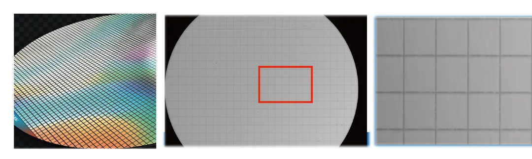
1、Wafer
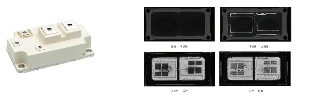
2、IGBT:
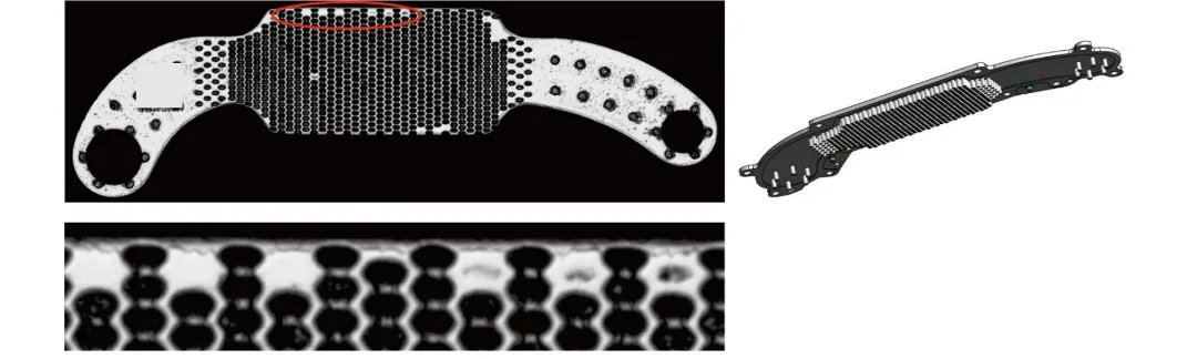
3、Liquid-Cooled Heatsink:
4、Chip:
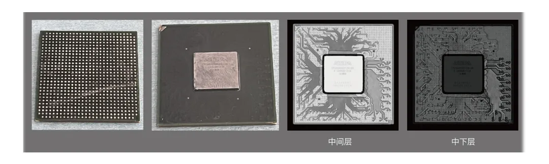
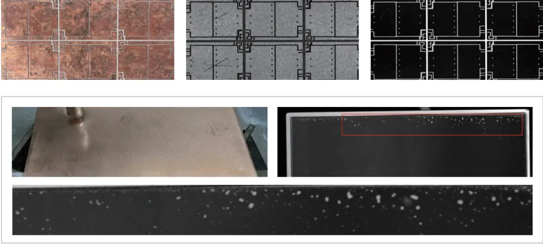
5、Ceramic Copper Clad Board AMB/DBC:
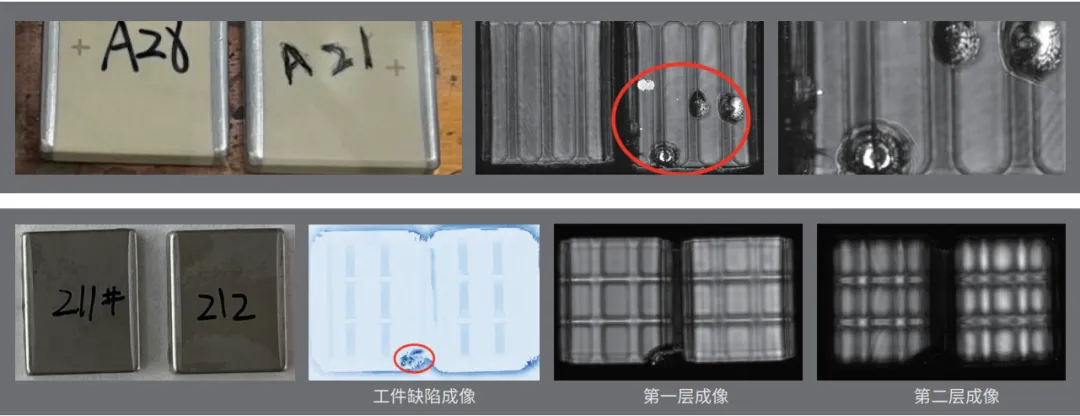
6、Multi-Layer Ceramic Capacitor (MLCC):
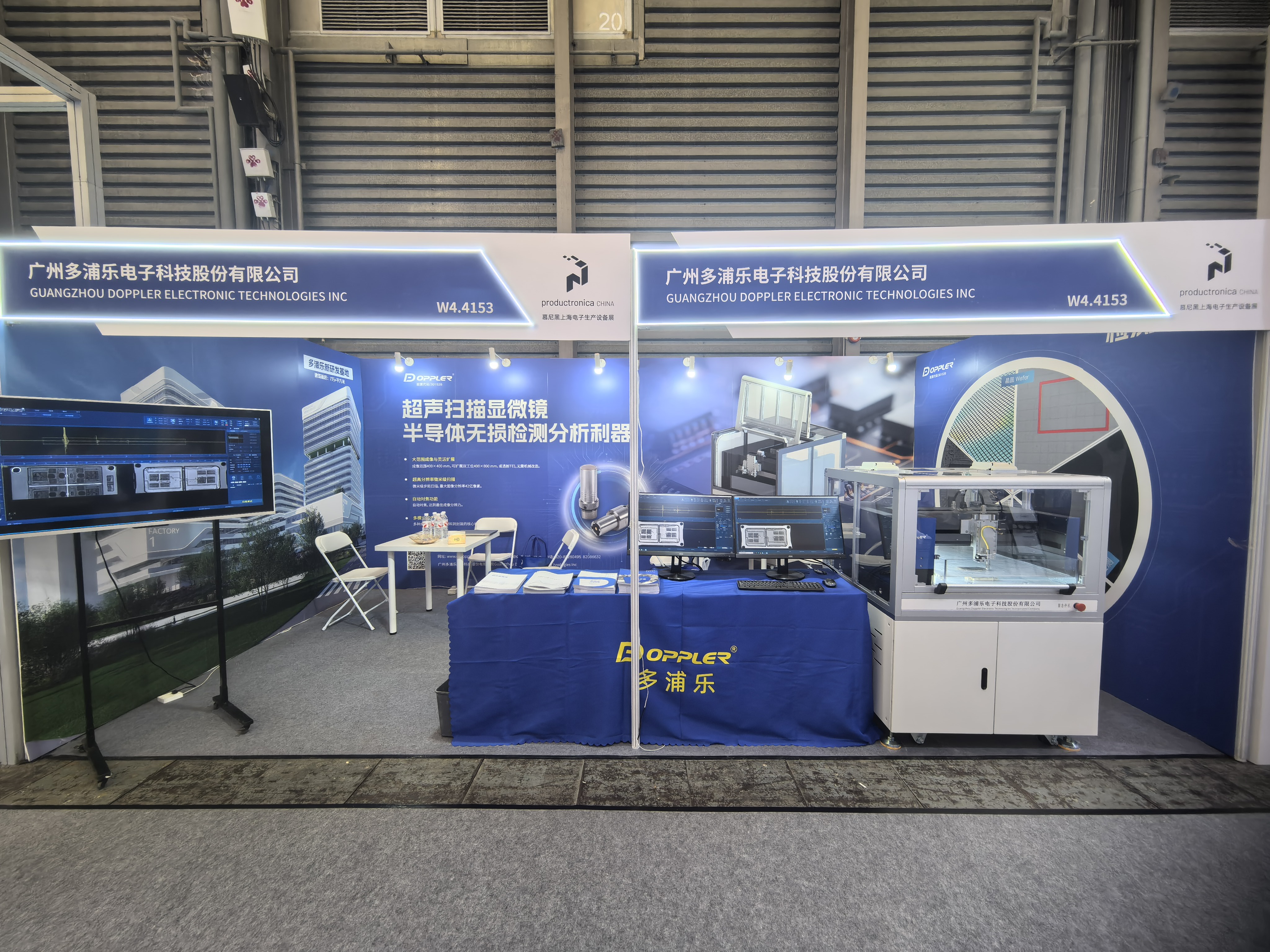
Doppler Booth
We would like to thank new and long-term customers for visiting the Doppler booth and recognizing our products with high praise. Moving forward, Doppler will steadily increase R&D investment in semiconductor non-destructive testing equipment. Through continuous technological innovation, product upgrading and iterative optimization, we will launch more high-performance devices to support the high-quality development of China’s semiconductor industry.